Caches
Caches buffer data to exploit the principle of locality, reducing average memory access time by keeping frequently used data closer to the processor. Memory requests that locate requested data in the cache are hits, while requests that fail to find data are misses.
- Temporal locality: If a data location is referenced, it will tend to be referenced again soon (e.g., loop variables).
- Spatial locality: If a data location is referenced, nearby addresses will tend to be referenced soon (e.g., sequential array elements).
Memory is organized as a memory hierarchy consisting of multiple levels.
- Higher levels (closer to the processor) are smaller, faster, and more expensive per bit.
- Lower levels are larger, slower, and cheaper per bit.
- Block (or line): The minimum unit of information transferred between two adjacent levels.
- Hit rate: The fraction of accesses found in the upper level; hit time is the time to access the upper level and determine the hit/miss status.
- Miss rate (): The fraction of accesses not found. Miss penalty is the time required to fetch the block from the lower level, insert it, and pass it to the requestor.
Cache operations are defined by four primary design questions:
Q1: Placement
Block placement determines where a fetched memory block can be stored in the cache.
- Direct-Mapped: Each memory block has exactly one valid cache location.
- Set Associative: The cache is divided into sets; a block maps to a single set but can be placed in any block frame within that set.
- Fully Associative: A block can be placed in any block frame within the cache.

Q2: Identification
Caches identify stored blocks using physical or virtual address partitioning.
- Address Fields: The processor address is partitioned into a Block Address (Tag + Index) and a Block Offset.
- Tag: Used to search all blocks in the selected set in parallel.
- Index: Used to select the specific cache set, minimizing the tag size. Fully associative caches do not use an index field.
- Valid Bit: Indicates whether the matched cache entry contains valid data.

Q3: Replacement
On a cache miss, a block must be evicted to make room for the newly fetched block.
- Least Recently Used (LRU): Evicts the block that has gone the longest without being accessed. Expensive to compute for high associativity.
- Pseudo-LRU: Approximates LRU using a set of bits per set to track recently accessed ways, randomly replacing a block from an un-accessed way.
- First In, First Out (FIFO): Evicts the oldest block in the set.
- Random: Evicts a randomly chosen block; simple to implement in hardware.
Q4: Write Strategy
Writes account for approximately 28% of data cache traffic and require tag verification before modification to prevent corruption.
- Write-Through: Data is written to both the cache block and the lower-level memory. Typically paired with a no-write allocate policy, where write misses update main memory directly without loading the block into the cache.
- Write-Back: Data is written only to the cache. The block is written to main memory only upon eviction, requiring a dirty bit to track modification. Typically paired with a write allocate policy, where write misses fetch the block into the cache before modification.
- Write Buffer: Used to prevent write stalls by overlapping processor execution with memory updates.
Performance Metrics
Evaluating cache performance relies on memory stall cycles and average access times rather than instruction count alone.
Stall Cycles
CPU execution time factors in stalls caused by the memory hierarchy:
Memory stall cycles are calculated based on cache miss rates:
AMAT
AMAT provides a normalized metric for memory hierarchy efficiency:
OOO Adjustments
Out-of-order processors can overlap memory latency with instruction execution. Miss penalty is redefined as the non-overlapped latency that stalls the processor:
Three Cs
Cache misses are categorized into three fundamental types to guide optimization strategies:
- Compulsory (Cold-Start): The first access to a block that has never been in the cache. These occur even in infinite-sized caches.
- Capacity: Occurs when the cache cannot hold all the blocks needed during program execution, causing active blocks to be discarded and retrieved (thrashing).
- Conflict (Collision): Occurs in set-associative or direct-mapped caches when multiple required blocks compete for the same set, leading to evictions that would not occur in a fully associative cache.
Six Basic Optimizations
Reducing Miss Rate
- Larger Block Size: Exploits spatial locality to reduce compulsory misses. Trade-offs: Increases miss penalty and may increase conflict/capacity misses if the block size is too large relative to cache size.
- Larger Caches: Directly reduces capacity misses. Trade-offs: Increases hit time, manufacturing cost, and static/dynamic power consumption.
- Higher Associativity: Reduces conflict misses. Follows the 2:1 Cache Rule of Thumb: A direct-mapped cache of size has roughly the same miss rate as a 2-way set-associative cache of size . Trade-offs: Multiplexing logic increases hit time and may slow down the processor clock.
Reducing Miss Penalty
-
Multilevel Caches: Introduces an L2 (or L3) cache to bridge the gap between fast L1 caches and slow main memory.
- AMAT for Two Levels:
- Global vs. Local Miss Rate: The local miss rate () is the fraction of misses in the L2 cache based only on L1 left-overs. The global miss rate () measures the fraction of total processor memory accesses that must go to main memory.
- Inclusion vs. Exclusion: Multilevel inclusion forces all L1 data to reside in L2, simplifying consistency checks. Multilevel exclusion ensures L1 data is never duplicated in L2, optimizing total capacity when L2 is only slightly larger than L1.
-
Giving Priority to Read Misses Over Writes: Allows a read miss to bypass queued writes in the write buffer, provided there are no address conflicts. This significantly reduces the read miss penalty and prevents stalls.
Reducing Hit Time
- Avoiding Address Translation During Indexing: Uses the page offset (which is identical in both virtual and physical addresses) to index the cache directly.
- Virtually Indexed, Physically Tagged Caches: Tag comparison overlaps with address translation. Requires the direct-mapped cache size to be the page size to function natively.
- Page Coloring: Software enforces constraints so that aliases share specific address bits, effectively increasing the page offset and allowing larger virtually indexed caches without physical address duplication (aliasing).
Virtual Memory
Virtual memory divides physical memory into blocks, allocating them to distinct processes to enable memory sharing and process protection.
- Relocation: The hardware dynamically maps virtual addresses to physical addresses, allowing a program to be loaded anywhere in physical main memory or secondary storage.
- Page Fault / Address Fault: Occurs when a referenced item is not present in main memory. The missing block is moved from disk to memory.
Page faults are managed entirely by the operating system (OS) in software. The processor performs a context switch to another task while the high-latency disk access completes.

Paging vs. Segmentation
- Paging: Divides the address space into fixed-size blocks called pages (typically 4–8 KBs).
- Addresses consist of a virtual page number and a page offset.
- Causes internal fragmentation (unused memory within an allocated page).
- Segmentation: Divides the address space into variable-size blocks called segments (ranging from 1 byte to bytes).
- Addresses require two distinct words: a segment number and an offset within the segment.
- Causes external fragmentation and makes block replacement difficult due to contiguous memory requirements.
- Hybrid Approaches:
- Paged segments: Segments are composed of an integral number of pages, simplifying replacement.
- Multiple page sizes: Supports base pages and larger sizes structured as powers of 2 multiples of the base size.

Four Hierarchy Questions
- Placement (Fully Associative): Because disk miss penalties are exorbitant, operating systems minimize miss rates by placing pages anywhere in main memory.
- Identification (Page Tables): The OS locates blocks using a data structure indexed by the virtual page number, yielding the physical page address.
- Paging: The offset is directly concatenated to the physical page address.
- Segmentation: The offset is added to the segment’s physical base address.
- Inverted Page Table: Applies a hashing function to the virtual address, reducing the page table size to the number of physical pages rather than virtual pages.
- Hierarchical Page Tables: To avoid allocating massive contiguous page tables (e.g., 64 billion entries for a 48-bit address space), architectures use multi-level tree structures, paging the page tables themselves.
- Replacement (Least Recently Used - LRU): The OS approximates LRU replacement to minimize page faults.
- Processors provide a use bit or reference bit that is set upon access.
- The OS periodically clears and records these bits to identify unreferenced pages for replacement.
- Write Strategy (Write-Back): Writes update main memory and are only written to disk upon replacement.
- A dirty bit tracks if the page has been altered, ensuring only modified blocks are written to the high-latency disk.

TLB
- Page tables reside in main memory. Address translation directly through a page table doubles memory access time (one access for translation, one for data).
- A TLB is a dedicated cache for address translations that bypasses the secondary memory access for the majority of references.
- TLB entries contain: a tag (virtual address bits), the physical page frame number, protection fields, a valid bit, a use bit, and a dirty bit.
- A dirty bit in the TLB indicates that the corresponding memory page has been modified, not that the TLB entry itself is modified.
Page Size
- Advantages of Larger Page Sizes:
- Decreases page table size.
- Permits larger virtually indexed caches.
- Increases secondary storage transfer efficiency.
- Reduces TLB misses by mapping more memory per entry.
- Advantages of Smaller Page Sizes:
- Reduces internal fragmentation (wasted memory within a page).
- Decreases process start-up time.
Protection Architecture
- A process consists of a running program and the state required to continuously execute it.
- Hardware architectures and operating systems must enforce four specific mechanisms to allow safe sharing of hardware:
- Execution Modes: The architecture must provide at least two modes to differentiate between a user process and a supervisor (kernel) process.
- Protected State: A user process must be restricted from modifying specific processor states, including the user/supervisor mode bit, exception enable/disable bits, and memory protection boundaries.
- Mode Transitions: Processors require special system call instructions that save the Program Counter (PC), transfer control to a dedicated supervisor address, and elevate privilege to supervisor mode.
- Memory Isolation: Mechanisms must restrict memory accesses to prevent user processes from modifying the memory state of other processes without relying on disk swapping during context switches.
Page Protection and TLBs
- Memory protection is heavily reliant on mapping fixed-sized virtual memory pages (e.g., or ) to physical addresses using a page table.
- Each Page Table Entry (PTE) contains protection restrictions determining if a user process can read, write, or execute the given page.
- Total access protection is guaranteed because a process cannot access a page missing from the page table, and only the operating system is permitted to update page table entries.
- Because paged virtual memory intrinsically requires two memory accesses (one for translation, one for data), TLBs cache address translations to preserve performance.
- A TLB entry stores a tag containing virtual address bits, alongside data fields holding the physical page address, protection restrictions, a valid bit, a use bit, and a dirty bit.
- When the operating system alters page restrictions, it modifies the page table and invalidates the corresponding TLB entry.
Protection and Sharing
- Process: A running program and its requisite execution state. Multi-programming requires rapid context switches between processes.
- Protection Boundaries: Dedicated page tables per process prevent unauthorized interference.
- Protection Rings: Concentric security levels. Inner kernel rings access all outward data; outer civilian rings have highly restricted access.
- Capabilities: Unforgeable keys explicitly passed between programs to securely grant access rights.
VM Architectures
IA-32: Segmented VM
- Protection Levels: Implements four levels of protection rings, utilizing separate stacks for each level to prevent security breaches.
- Descriptor Tables: Segment registers hold an index to a descriptor table rather than a base address. Half the address space is shared (Global Descriptor Table) and half is private (Local Descriptor Table).
- Segment Descriptors (PTE equivalent): Contain a Present bit, Base field, Access bit, Attributes, and a Limit field that enforces strict upper-bound offset checks.
- Call Gates: Special segment descriptors that define strictly controlled entry points for executing more privileged code.
- Call gates safely transfer parameters across privilege boundary stacks based on a descriptor’s word count field.
- Hardware sets a requested privilege level field to prevent the OS from utilizing trusted access on behalf of untrusted parameters.
AMD64: Paged VM
- Address Space: Utilizes a flat, 64-bit address space with segment bases set to zero. Implements 48-bit virtual addresses mapped to 40-bit physical addresses.
- Canonical Form: Hardware requires the upper 16 bits of a virtual address to be the sign extension of the lower 48 bits.
- Page Tables: Employs a 4-level hierarchical page table structure. Each table fits exactly within a 4 KiB page.
- Page Table Entry (PTE): 64-bit entries containing a 52-bit physical page frame and 12 bits of state.
- State fields include: Presence, Read/Write, User/Supervisor, Dirty, Accessed, Page Size, No Execute, Cache Disable, and Write-Through.
- TLB Hierarchy: Uses four TLBs (two L1 and two larger L2 structures) separated for instructions and data to minimize the translation penalty incurred by 4-level page walks.
Cache-VM Interaction
Virtual Caches
Virtual caches use virtual addresses for both the index and the tag comparison, eliminating address translation time on a cache hit.
- Challenges of Virtual Caches:
- Context Switches: Virtual addresses map to different physical addresses across processes, typically requiring cache flushes.
- Aliasing/Synonyms: Multiple virtual addresses mapping to the same physical address can result in inconsistent data copies within the cache.
- Solutions:
- Process-Identifier Tags (PID): Appending a PID to the cache tag allows the cache to retain data across process switches without flushing.
- Antialiasing Hardware: Guarantees a unique physical address for every cache block.
- Page Coloring: Software restricts aliases to share identical lower address bits, effectively increasing the page offset.
VIPT Caches
- VIPT caches use the page offset (which is identical in both virtual and physical addresses) to index the cache.
- The virtual portion of the address is translated by the TLB in parallel with the cache read. The resulting physical address is used for the tag comparison.
- Sizing Constraint: A direct-mapped VIPT cache cannot exceed the page size. To support a larger cache without translating the index, associativity must be increased according to the index formula:
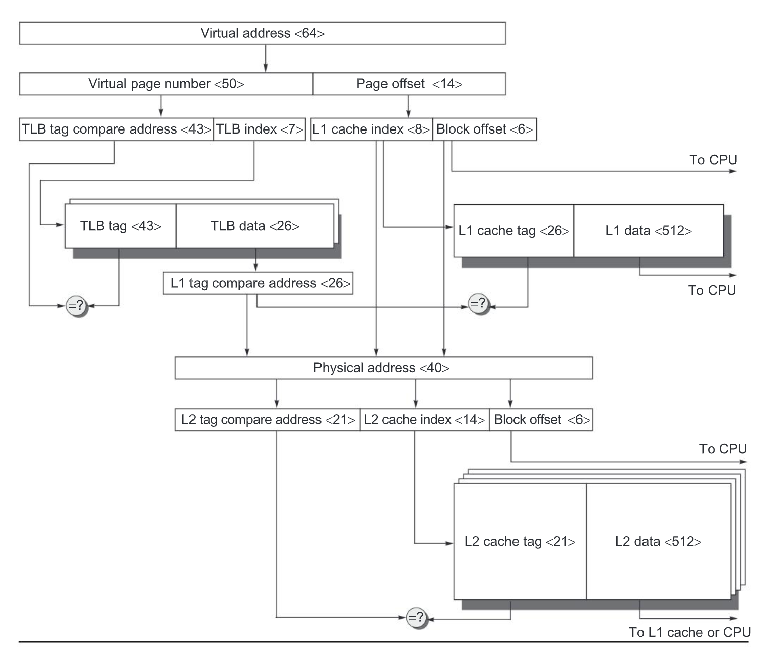
The overall picture of a hypothetical memory hierarchy going from virtual address to L2 cache access. The page size is 16 KiB. The TLB is two-way set associative with 256 entries. The L1 cache is a direct-mapped 16 KiB, and the L2 cache is a four-way set associative with a total of 4 MiB. Both use 64-byte blocks. The virtual address is 64 bits and the physical address is 40 bits.
Side-Channel Attacks
- Functional isolation enforced by page tables and operating systems can be circumvented via hardware side-channels.
- Side-channel attacks perturb shared hardware components not explicitly protected by virtual memory (e.g., caches) and observe the effects using processor timers or performance counters.
- Prime and Probe Attack:
- Given target logic:
if (x < 0) {access P} else {access Q}. - Prime: The attacker overwrites cache lines corresponding to locations and with its own data.
- Execute: The victim executes the target logic, generating a cache miss and loading either or into the shared cache.
- Probe: The attacker accesses and while measuring access times.
- A cache miss on indicates the victim’s code execution replaced the attacker’s data at , definitively leaking the state .
- Given target logic:
- Attack Requirements and Amplifiers:
- The attacker must know the precise memory locations of the victim’s code.
- The victim must execute between the prime and probe steps without intervening actions polluting the cache.
- Shared Last-Level Caches (LLC) across multi-core processors, or hardware multithreading within the same core, drastically increases the bandwidth and effectiveness of side-channel attacks.
Mitigations
- Randomized Page Allocation: Allocating pages randomly complicates the attacker’s ability to map victim code segments to specific physical cache locations.
- Timing Obfuscation: Inserting random, short computational delays into critical code segments masks the timing signals relied upon by attackers.
- Cache Flushing: Flushing caches entirely upon context switches eliminates implicit sharing but incurs severe performance penalties on large LLCs.
- Resource Partitioning: Dividing the LLC into discrete segments for simultaneously active processes stops cache state leakage, though it reduces performance for memory-heavy applications.
Cache Coherency
- Memory inconsistencies occur when multiple processors or I/O devices interact with shared cached data.
- Multiprocessor Coherency: Shared-memory multiprocessors must maintain consistent copies of the same data across multiple distinct caches.
- I/O Coherency: Interactions between I/O devices and memory require strict management to prevent reading or writing stale data.
- I/O via Cache: Routing I/O directly through the cache guarantees consistency but stalls the processor and evicts valuable cache blocks,.
- I/O via Main Memory: Routing I/O to main memory (acting as an I/O buffer) avoids processor interference but requires mechanisms to handle stale cache data.
- Write Policies: Write-through caches natively keep main memory updated, but modern memory hierarchies typically pair write-through L1 caches with write-back L2 caches,.
- Write Merging Limitations: Memory-mapped I/O registers demand precise single-address accesses and fail if writes are merged. Hardware handles this by marking specific I/O pages as requiring nonmerging write-through,.
- Software Invalidation (Input): Operating systems prevent stale data by marking I/O input pages as noncacheable or by explicitly flushing targeted buffer addresses before input occurs,.
- Hardware Invalidation (Input/Output): Hardware dynamically checks I/O addresses against cache tags, invalidating matching cache entries to guarantee memory consistency.
Advanced Optimizations
Advanced memory hierarchy optimizations address the processor-memory performance gap by targeting specific components of the average memory access time (AMAT) equation and system power consumption.
Optimizations are classified into five core categories:
- Reducing hit time and power consumption: Smaller caches and multibanked structures.
- Increasing cache bandwidth: Pipelined caches, multibanked caches, and nonblocking caches.
- Reducing miss penalty: Critical word first, merging write buffers, and multibank/High Bandwidth Memory (HBM).
- Reducing miss rate: Compiler optimizations and optimized associativity.
- Reducing miss penalty or miss rate via parallelism: Hardware and compiler prefetching.
1. Pipelined L1 Caches
Pipelining the Level 1 (L1) cache enables higher processor clock rates at the cost of slightly increased cache latency (e.g., 4 cycles for an instruction cache access).
- Standard Pipeline Stages:
- Address decode to select the word line.
- Access the SRAM array.
- Compare tags against the physical tag from the Translation Lookaside Buffer (TLB) to determine hit/miss.
- Multiplex the block and transmit data.
- Way Prediction: Reduces the energy and hit time of set-associative caches to match direct-mapped caches. Extra bits predict the specific “way” (block within a set) of the next access. The multiplexor is set early, requiring only a single tag comparison per cycle. A misprediction requires checking the remaining blocks in the next cycle.
- Victim Caches: Small caches that hold recently evicted lines to reduce the miss rate of direct-mapped L1 caches. Modern designs often rely on higher L1 associativity and prefetching instead.
2. Multibanking and Ports
Multiple-issue processors require data caches to service multiple memory references per clock cycle.
- Banking: The cache is divided into independent banks. Block addresses are interleaved across banks sequentially. This allows multiple parallel accesses provided they target different banks.
- Dual-Porting vs. Banking: Dual-porting directly increases bandwidth but increases cache access time and area. A multibanked cache with dual ports on each bank reduces the probability of collisions (three concurrent references to the same bank are required to cause a stall).
3. Advanced Replacement Policies (Pseudo-LRU)
Higher associativity requires sophisticated replacement policies to minimize miss rates without the hardware overhead of strict Least Recently Used (LRU) tracking.
- Not Recently Used (NRU): A 1-bit per element pseudo-LRU scheme. The bit is cleared on access. On a miss, a block with an active NRU bit is replaced, and all other bits in the set are reset. Replaces randomly if all bits are active.
- Recently Referenced Prediction Counter: Uses a saturating counter (e.g., 2-bit) per block. Set to 0 on a hit. On a miss, if any block equals the maximum value (e.g., 3), it is replaced. Otherwise, all counters increment. This explicitly distinguishes streaming accesses (used once) from data with high temporal locality.
4. Multibanked L2 and L3 Caches
Extending banking to Last Level Caches (LLC, such as L2 and L3) improves performance and power characteristics.
- Power Reduction: Accessing a single bank instead of the entire cache array reduces dynamic power consumption.
- Bandwidth: Increases the refill bandwidth necessary to support nonblocking L1/L2 caches.
5. Nonblocking Caches
Out-of-order (OOO) processors do not need to stall immediately on a data cache miss. Nonblocking (or lockup-free) caches continue to supply data for subsequent hits during a miss (“hit under miss”).
- Miss Under Miss: Modern memory systems overlap multiple outstanding misses to further hide latency.
- Miss Status Handling Registers (MSHR): Hardware structure used to track outstanding misses. MSHRs record the requesting instruction, the destination physical register, and the cache block location. When data returns, the MSHR routes the data, updates the cache, and notifies the scheduler to wake up dependent instructions.
6. Critical Word First and Early Restart
Processors typically require a single word from a block to continue execution. These optimizations bypass waiting for the full block transfer to reduce the effective miss penalty.
- Critical Word First: The memory system prioritizes fetching the specifically requested word, passing it immediately to the processor, and filling the remainder of the block in the background.
- Early Restart: The block is fetched in normal sequential order. Once the requested word arrives, it is forwarded to the processor to resume execution.
7. Compiler Optimizations
Compilers reorder instructions and data accesses to explicitly improve spatial and temporal locality without hardware changes.
- Loop Interchange: Swapping nested loops to align the access pattern with the memory layout. For example, changing a column-major access pattern to a row-major access pattern ensures sequential words are accessed within the same cache block, directly reducing capacity misses.
- Cache Blocking: Operating on submatrices () instead of entire rows or columns. This keeps a subset of the data continuously resident in the cache, maximizing temporal locality. For multiplying matrices, blocking reduces memory accesses from to .
8. Hardware Prefetching
Hardware predicts future data and instruction needs, fetching them into the cache or a separate buffer before they are requested.
- Instruction Prefetch: Fetches the requested block and the subsequent sequential block. The sequential block is placed in an instruction stream buffer.
- Data Prefetch: L2 data prefetchers often fetch data directly from L3 or memory into the L2 cache. Effective prefetching converts L3 misses into L2 hits, dramatically reducing latency.
- Trade-offs: Prefetching increases overall memory traffic. Inaccurate prefetches displace useful data (cache pollution) and waste bandwidth, negatively impacting power consumption.
9. Compiler-Controlled Prefetching
Compilers explicitly insert prefetch instructions to load data ahead of use.
- Prefetch Types: Can be directed to a register or directly into the cache.
- Non-faulting (Non-binding): Modern implementations use non-faulting instructions; if the prefetch generates a virtual memory fault or protection violation, it safely executes as a no-op.
- Implementation: The compiler unrolls loops and schedules prefetch instructions to overlap the memory latency with useful execution. Requires nonblocking caches.
10. Multiple Memory Buses and HBM
High-speed processors use multiple memory channels to increase bandwidth and prevent independent accesses from stalling one another.
- NonUniform Memory Architecture (NUMA): Systems mix standard SDRAM and High Bandwidth Memory (HBM). Software or domain-specific languages explicitly manage data placement in the faster HBM.
- HBM as Last Level Cache (L4): Using HBM as an massive cache introduces a tag storage problem. Storing tags in SRAM requires enormous area (e.g., 96 MiB of tags for a 1 GiB cache).
- Alloy Cache: Molds the tag and data together within the HBM using a direct-mapped structure. A single HBM burst transfers both tag and data, completing the LLC access in one cycle. A miss predictor avoids the latency of the initial HBM tag access if the request is highly likely to miss.
ARM Cortex-A53
Architecture Overview
- Target Domain: Personal Mobile Devices (PMDs) such as tablets and smartphones, prioritizing high energy efficiency.
- Core Delivery: Distributed as a configurable Intellectual Property (IP) core rather than a fixed hardware chip.
- Hard Cores: Optimized for specific semiconductor vendors, providing higher performance and smaller die area, but limited to external parameterization (e.g., L2 cache size).
- Soft Cores: Built using standard logic libraries, allowing extensive modification and retargeting across different semiconductor vendors.
- Processor Base: Dual-issue, statically scheduled superscalar core supporting the ARMv8A ISA (32-bit and 64-bit modes) with clock rates up to 1.3 GHz.
Memory Hierarchy
The memory system relies on a two-level Translation Lookaside Buffer (TLB) and a two-level cache structure.
Translation Lookaside Buffers (TLBs)
- Instruction MicroTLB: 10 entries, fully associative, 2-clock-cycle miss penalty.
- Data MicroTLB: 10 entries, fully associative, 2-clock-cycle miss penalty.
- L2 Unified TLB: 512 entries, 4-way set associative, 20-clock-cycle miss penalty.
- Optimization: A dedicated page map cache tracks physical page locations for a set of virtual pages, directly reducing the L2 TLB miss penalty.
L1 Caches (Instruction and Data)
- Capacity: Configurable from 8 KiB to 64 KiB.
- Organization:
- Instruction Cache: 2-way set associative, 64-byte block size.
- Data Cache: 2-way or 4-way set associative, 64-byte block size.
- Indexing & Tagging: Virtually indexed, physically tagged.
- Miss Penalty: 13 clock cycles (latency to retrieve from L2).
- Miss Handling:
- The critical word is returned first to immediately resume processor execution.
- Nonblocking architecture allows the processor to continue operating while the miss completes.
- Write Policy (Data): Write-back policy, defaulting to allocate-on-write.
- Replacement Policy: Least Recently Used (LRU) approximation.
L2 Unified Cache
- Capacity: Configurable from 128 KiB to 2 MiB.
- Organization: 16-way set associative, 64-byte block size.
- Miss Penalty: 124 clock cycles (latency to retrieve from main memory).
- Write Policy: Write-back policy, defaulting to allocate-on-write.
- Replacement Policy: LRU approximation.
- Main Memory Interface: Connects to main memory via a 64-bit to 128-bit wide bus, supporting up to 4 memory banks.
Memory Addressing
Virtual address spaces are partitioned to index the TLBs and caches sequentially.
-
Cache Indexing Calculation:
-
Aliasing Challenge: When the cache index plus the block offset exceeds the page offset, a single physical page can map to multiple cache addresses.
- Example: With a 32 KiB 2-way set associative L1 cache and 64-byte blocks, the index size is 8 bits.
- Given a 4 KiB page size (12-bit page offset) and a 6-bit block offset, the index uses 14 bits of the address ().
- This forces 2 bits of the virtual page number to overlap with the cache index, creating potential aliases.
-
Resolution: Hardware dynamically detects and prevents aliases during cache miss processing to maintain data consistency.
Performance Characteristics
System performance heavily depends on application memory footprints and the extreme disparity between L1 and L2 miss penalties.
- L1 Instruction Cache: Consistently achieves near-zero miss rates (under 1%) across standard benchmarks like SPECInt2006.
- Data Caches: Miss rates are highly application-dependent. Benchmarks with large memory footprints (e.g.,
mcf) generate significantly higher miss rates in both the L1 data cache and the L2 global cache. - Average Memory Access Penalty: Even when L1 miss rates are high, the overall average memory access penalty is dominated by L2 misses. The architectural penalty for accessing main memory (124 cycles) overwhelms the L1 miss penalty (13 cycles), emphasizing the necessity of high L2 hit rates for optimal PMD battery life and processor speed.
Intel Core i9 12900 (Alder Lake)
Architecture Overview
- Microarchitecture: Alder Lake (big.little design).
- Core Configuration: 8 Performance cores (P-cores) and 8 Efficiency cores (E-cores). P-cores support multithreading and reach peak clock rates of 5.1 GHz in Turbo Boost mode.
- Bandwidth Demands: Capable of generating up to four 128-bit data memory references per core per clock cycle. At 3 GHz, 8 cores demand a peak bandwidth of 3840 GiB/s.
- Main Memory Interface: Dual memory channels supporting DDR4 or DDR5. Maximum bandwidth with DDR5-4800 is 77 GB/s.
Translation Lookaside Buffer
- Address Space: 48-bit virtual address space mapped to a 36-bit physical address space.
- Translation Hierarchy: Utilizes a two-level TLB structure.
- Instruction TLB (L1 I-TLB):
- 256 entries for 4 KiB pages; 32 entries for 2/4 MiB pages.
- 8-way set associative; Pseudo-LRU replacement.
- 1-cycle access latency.
- Data TLB (L1 D-TLB):
- 96 entries for 4 KiB pages; 32 entries for 2/4 MiB pages; 8 entries for 1 GiB pages.
- 6-way, 4-way, and 8-way set associative (varies by page size); Pseudo-LRU replacement.
- 1-cycle access latency. Includes separate structures for loads and stores.
- Second-Level TLB (STLB):
- 2048 entries supporting 4 KiB, 2 MiB, and 1 GiB pages.
- 16-way set associative; Pseudo-LRU replacement.
- 8-cycle access latency (9-cycle total miss penalty from L1 TLB).
- Instruction TLB (L1 I-TLB):
- Page Table Walker: Hardware-based page table walker handles STLB misses, supporting up to four parallel page table walks.
Cache Hierarchy
All cache levels utilize a 64-byte block size and employ write-back policies (where applicable).
- L1 Instruction Cache (L1I):
- Size: 32 KiB per core.
- Associativity: 8-way set associative.
- Latency: 4 clock cycles.
- Addressing: Virtually indexed, physically tagged.
- L1 Data Cache (L1D):
- Size: 48 KiB per core.
- Associativity: 6-way set associative (dual-ported).
- Latency: 5 clock cycles.
- Addressing: Virtually indexed, physically tagged.
- L2 Cache:
- Size: 1.25 MiB per P-core.
- Associativity: 10-way set associative.
- Latency: 15 clock cycles.
- Addressing: Physically indexed, physically tagged.
- Replacement: Weighted n-bit LRU.
- L3 Cache (Last Level Cache - LLC):
- Size: 30 MiB shared across all cores.
- Structure: Distributed into 8 banks. A hash function maps addresses to specific banks.
- Associativity: 15-way set associative.
- Latency: 50 clock cycles.
- Inclusion Policy: Non-inclusive. Primarily holds blocks ejected from the L2 cache.
Memory Access Flow
The 64-bit virtual address resolves to a 36-bit physical address. Cache access relies on splitting the physical address into Tag, Index, and Block Offset.
- Block Offset: All caches use 64-byte blocks, requiring a 6-bit offset ().
- L1 Instruction Cache Access:
-
Index:
-
Tag:
-
Fetch Width: The fetch unit retrieves 32 bytes per cycle. It uses 1 additional bit from the 6-bit block offset to select the correct 32-byte chunk.
-
- L2 Cache Access:
-
Index:
-
Tag:
-
- L3 Cache Access (Per 3.75 MiB Bank):
-
Index:
-
Tag:
-
Cache Miss and Write Management
- L1 Data Cache Write Strategy:
- Utilizes a no-write-allocate policy on write misses.
- Store misses bypass cache allocation and are placed directly into a merging write buffer.
- Merging Write Buffers:
- Captures dirty cache lines and unallocated write misses.
- Writes data back to the next memory level when that level is not actively serving a read request.
- Checked concurrently during a cache miss; if the requested line resides in the write buffer, the miss is filled directly from the buffer.
- L3 and Main Memory Interaction:
- A miss at the L3 cache initiates a main memory access.
- Miss Penalty: ~50 cycles to detect the L3 miss + ~160 cycles DRAM latency (DDR5-4800) 200 cycles for the first 16 bytes. The remaining 48 bytes transfer at 32 bytes/cycle, taking 10 additional cycles.
- Due to the non-inclusive policy, data fetched from main memory is written directly into L1 and L2 caches, bypassing L3 insertion.
- Hardware Prefetching: Supported at both L1 and L2 levels, predicting and fetching data from the next level in the hierarchy to hide latency.
Performance Metrics
- Miss Rates (MPKI):
- Instruction cache miss rates remain highly optimized (<1% for most integer workloads).
- Memory-intensive workloads generate significant L1D misses (>20 MPKI) and L2 misses (>10 MPKI), placing heavy reliance on the L3 cache and hardware prefetchers.
The full Intel Core i9-12900 (Alder Lake) memory hierarchy, illustrating how all the concepts above — VIPT caches, multilevel TLBs, non-inclusive LLC, write buffers, and hardware prefetchers — come together in a real processor.
